- 20th INTERNATIONAL SYMPOSIUM "NANOSTRUCTURES: PHYSICS AND TECHNOLOGY"
- Nanotech Europe 2009
- SMART SYSTEMS INTEGRATION 2009
- The 14th Canadian Semiconductor Technology Conference (CSTC-2009) and the 4th Nano & Giga Forum (NGC-2009 - Nano & Giga Challenges in Electronics, Photonics, and Renewable Energy).
- http://www.ioffe.ru/natoarw/2009/ 29 June –02 July, 2009
- Design, Test, Integration & Packaging of MEMS/MOEMS
- V МЕЖДУНАРОДНАЯ ВЫСТАВКА NTMEX 08
- 5th International Technology Transfer Days BIOMATERIAL 2009
- COMS - Commercialization of Micro and Nano Systems Conference, 31st August - 4th September 2008, Puerto Vallarta, Mexico
- ICCE - Integration and Commercialization of Micro and Nanosystems International, 3rd - 5th June 2008, Hong Kong, China
- The Fourth International Conference on "Science and Business": NanoBio and Related New and Perspective Biotechnologies Pushchino Biological Center of Russian Academy of Sciences Moscow Region, Russia, October 15 - 18, 2007.
- MicroNanoWorld
- SYMPOSIUM on Design, Test, Integration and Packaging of MEMS/MOEMS
- Micro-Nano Technologies for Aerospace Applications From Concepts to Systems.
- 20th Eurosensors Conference Anniversary
- Symposium and School on Nano
and Giga Challenges in Electronics and Photonics:
from Atoms to Materials to Devices
to System Architecture - MEMS & MST Conference
- I A R P
International Advanced Robotics Programme - 10th International Conference on the Commercialization of Micro and Nano Systems
COMS 2005 - ICMNE 2005 QI-2005
International Conference “Micro-& nanoelectronics-2005”
and International Symposium “Quantum Informatics – 2005” - Symposium on Design, Test, Integration and Packaging of MEMS / MOEMS
- International Congress of Nanotechnology 2004
- PEM-2004
Ninth International Science Conference
"Actual Problems of Solid-State Electronics and Microelectronics" - Int'l Workshop on MEMS and NANOTECHNOLOGY INTEGRATION (MNI): APPLICATIONS
- NATO
Advanced Research Workshop
Science and Technology of Semiconductor-On-Insulator structures and devices operating in a harsh environment - Symposium on Desigen, Test, Integration and Packaging of MEMS / MOEMS 2004
- European Micro and Nano systems 2004
- MANCEF - Micro and Nanotechnology Commercialization Education Foundation
- IEE Proceedings – Science, Measurement and Technology
- 10th Saint Petersburg international conference on integrated navigation systems
- 11th International Symposium «NANOSTRUCTURES: PHYSICS AND TECHNOLOGY»
- Word Microtechnologies Congress "MICRO.tec 2003"
- Nanotechnology Conference and Tradeshow "NanoTech 2003"
- International conference on microrobots, micromachines and microsystems
- Design, Test, Integration and Packaging of MEMS / MOEMS
- IV International scientific-technical conference "Electronics and information science - 2002"

|
NATO
Advanced Research Workshop
|

|
Science and Technology of
Semiconductor-On-Insulator structures and
devices operating in a harsh environment
|
|
|
25-29 April 2004, Kyiv, Ukraine
|
Workshop Chairmen:
Denis Flandre
Catholic University of Louvain,
DICE, Place du Levant, 3,
1348 Louvain-la-Neuve,
BELGIUM
Phone: 32.10.478135
Fax: 32.10.472598
E-mail: flandre@dice.ucl.ac.be
|
Alexei N. Nazarov
Inst. of Semiconductor Physics,
NAS of Ukraine
Prospekt Nauki 45,
03028 Kyiv-28
UKRAINE
Phone: 380(44) 2657022
FAX: 380(44) 2656177
E-mail: nazarov@lab15.kiev.ua
|
If you are planning to attend the workshop, please contact with organizers at your earliest convenience.
- Characterization of SOI materials and devices at extreme conditions
- SOI sensors
- Technology and economics
List of Keynote Speakers (with paper title):
Prof. F. Balestra (IMEP-ENSERG, Grenoble, France)
Reliability and electrical fluctuations in advanced SOI CMOS devices.
Dr. H. MORICEAU (LETI, Grenoble, France)
Advanced Smart-cut applications
Prof. S.Cristolovianu (ENSERG, Grenoble, France).
Electrical characterization of SOI structures and devices
Prof. D.Flandre (UCL, Louvain-la-Neuve, Belgium)
Recent fully-depleted SOI MOSFET advances
Prof. V.Bayot (UCL, Louvain-la-Neuve, Belgium)
Low-temperature SOI nanoelectronics
Dr. Dr. Valentin Nakov (IMMS, Germany)
Silicon-on-insulator circuits for application in a harsh environment
Dr. Dr. David Flores ( CNM, Spain)
High-voltage SOI transistors
Prof. S.Hall (University of Liverpool, UK)
SiGeOI devices and circuits
Dr. C.Johnston (HITEN, UK)
Development of high-temperature electronics in EC
Prof. F.Gamiz (Granada University, Spain)
Monte Carlo simulation of SOI devices
Prof. J.P.Colinge (UC Davis, USA)
Use SOI pi-MOSFETs for operation in hard conditions
Prof. C.Colinge (California State University, Sacramento, USA)
Achievements of low-temperature wafer bonding technology
Prof. W.Skorupa (Rossendorf Research Sentre, Dresden, Germany)
SiC-on-SOI by energy beam transient processing
Prof. J.Olsson (Uppsala University, Sweden)
High-voltage SOI devices for automotive application
Dr. Y.Ishikawa (Japan Fine Ceramics Center, Japan)
Achievements of SiGe-on-insulator technology
Prof. V.N.Mordkovich (Institute of Microelectronics Technology, Moscow, Russia)
Microelectronics SOI elements operating at harsh conditions
Dr. V.Popov (Institute of Semiconductor Physics, RAS, Novosibirsk, Russia)
SOI nanotransistors and their properties
Prof. V.N.Murashov (MISA, Moscow, Russia)
Functional-integrated electronics on SOI
Prof. V.P.Bondarenko (BSUIR, Minsk, Belorus)
Porous silicon based SOI: history and prospects
Prof. V.S.Lysenko (ISP, Kyiv, Ukraine)
Electron processes in SOI interfaces at cryogenic temperature
Prof. V.G.Litovchenko (ISP, Kyiv, Ukraine)
Simulation of SOI and SiC layer structures formation, using interstitials defects flow.
Workshop key dates
Deadline for Abstracts - 15 January 2004
Notification to Authors - 1 February 2004
Issue Preliminary Programme - 1 February 2004
Deadline hotel reservations - 15 March 2004
Arrival and welcome party - 25 April 2004
Call for Papers
We encourage the submission of papers related to the topics of the
Workshop. The proceedings of the Workshop will be published by
Kluwer Academic Publishers in the book “Science and Technology
of Semiconductor-On-Insulator structures and devices operating
in a harsh environment”. Only high-quality papers, containing
new and valuable results, will be accepted for publication after
a refereeing process. The typing instructions for the proceedings
will be sent together with the scientific programme of the workshop.
Abstracts:
Deadline: 15 January 2004
The abstract must be clearly typewritten or laser-printed on white paper
(size A4) with 2cm margins on the top, bottom, right sides and 3 cm margin on
left side. The abstract should be headed by the title (bold), author(s)
and affiliation. Please, identify the contact (presenting) author
with tel/fax number and e-mail address. Comprehensive
instruction for abstract preparation see on the last page of this
announcement.
The abstract should be submitted electronically to the following address:
houk@lab15.kiev.ua
GENERAL INFORMATION:
Historic Kyiv
Kyiv is the capital of the Ukraine with a population of about three million.
It is located about 400 km north of the Black Sea and lies on both East and West
banks of the River Dnipro which flows into the Black Sea. The Ukraine is a founding
member of the United Nations. The country declared its independence in 1991.
The city's history can be traces back to the fifth century but its rich heritage
principally dates from the eleventh century after the arrival of Christianity and
construction of cathedrals and monasteries. Much rebuilding has taken place and
today one can visit St Sophia's Cathedral (since 1990 a UNESCO World Heritage site),
The Golden Gate (memorable from Mussorgsky's "Pictures of an Exhibition"), St Cyrils
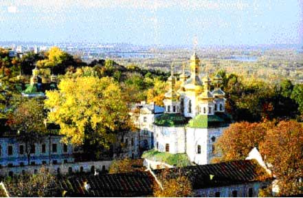
Church (twelfth century frescos), Kyiv-Pechersk Lavra (complex of buildings including
The Gate Church of the Trinity and caves) and more recent buildings including St
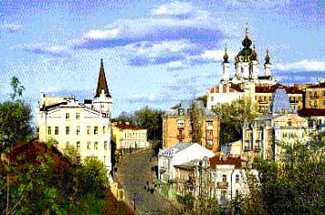
Volodymir's Cathedral (nineteenth century), St Andrew's Church (eighteenth century,
Baroque) and The Mariinski Palace, built during the eighteenth century. The city
has many other historic churches, museums, an opera house and the newly restores
National Philharmonic concert hall.
It is difficult to describe Kyiv in words. If you visit it, you will see for
yourself how beautiful and exciting it is. We are convinced that it will not
disappoint you, and you will be going back home full of new and unforgettable
impressions.
|
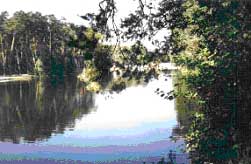
Venue
The Workshop venue is a sanatorium, which is located in picturesque woodlands
about 20 km of Kyiv city centre. The lecture theatre, meeting rooms, restaurant
and “en-suite” accommodation plus a bar/coffee shop are all located in adjacent
buildings within the
complex. A large lake, which is used for outdoor swimming during the summer,
is located within the grounds. Alongside the accommodation building is a resurfaced
tennis court which will be available for use by Workshop attendees.
The address of the venue is: Sanatorium "Puscha Ozerna",
Urban Settlement Puscha Voditsa, 14th line, Kyiv-75, Ukraine.
During the period of the Workshop attendees will have access to e-mail,
fax and telephone services which will be installed in the Workshop secretariat
in the sanatorium. Word processing (PC) and photocopying facilities will be
available, also.
|
Workshop Office
Prior and during the Workshop all communication should be directed to:
Yuri Houk
Inst. of Semiconductor Physics, NAS of Ukraine
Prospect Nauki 45,
03028 Kyiv-28
Ukraine
Phone: 380 44 265 7022
Fax: 380 44 265 6177
E-mail: houk@lab15.kiev.ua
Transportation
Kyiv, the capital of Ukraine, is easily accessible by air and train. There are direct
flights from European capitals.
The travel time by road from Borispol airport to Kyiv is about forty minutes (motorway) and,
also, about forty minutes from Kyiv city centre to the sanatorium, depending upon traffic
density.
Currency
The currency unit in the Ukraine is the Hryvnia (Hr).
The approximate exchange rates are (November 2004): 1$ (US) = 5.45 Hr; 1€ = 6.30 Hr.
Numerous currency exchanges are available in Kyiv.
Credit cards are not used extensively, however the larger hotels and stores will
accept them where Mastercard and Visa seems to be the preferred card.
Essentially, there is no limit to the amount of foreign currency and travellers
cheques that can be taken into the Ukraine but it is important to make a declaration
at the point of entry into the country (appropriate documents are available within
the Airport terminal).
Visa
Attendees from NATO and Western European countries and Japan will require entry visa.
Upon request from attendees, the Workshop organizers will provide "official"
letters of invitation which should be presented to the appropriate Ukrainian Embassy
together with a completed visa application from.
Social events
Sunday, April 25
Welcome reception will be held in the late afternoon in connection with registration at the restaurant of Sanatorium "Puscha-Ozerna".
Tuesday, April 27
Poster buffet with beer
Wednesday, April 28
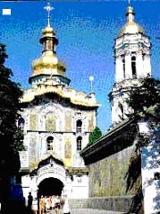
A guided tour to Kyiv-Pechersk Lavra - the ensemble of buildings with a Near and Far caves.
It was created throughout nine centuries and includes architectural monuments from the
11th to the 19th centuries. Now it is not only museum, but also a monastery.
REGISTRATION
Registration fee
The full registration fee (€80) for participants includes participation in the scientific
sessions, program booklet, abstract book, coffee breaks, social events like, e.g. excursion,
conference banquet, etc.
Registration fee should be paid in cash (Euro) in day of registration at the Registration desk.
Accommodation
As a service for the participants, the Local Committee will pre-book accommodation in
Sanatorium "Puscha Ozerna" for the period of April 25 to April 29, 2000 (5 nights).
The rate for lodging in a single room and full board is about €40 per day; the rate for
lodging in a double room and full board is about €35 per person and day.
In order to fulfill your requirements, you are advised to contact with Organizers at your
earliest convenience.
Workshop timetable
|
|
AM
|
1230-1400
|
PM
|
1830 - 2000
|
|
Sunday 25th Apr.
|
Registration
|
L
|
Registration
Welcome reception
|
D
|
|
Monday 26th Apr.
|
Opening
Technology and Economics
SOI Material Technologies
|
U
|
SOI Material Technologies
|
I
|
|
Tuesday 27th Apr.
|
Reliability and operation of
SOI devices in harsh enviroment
|
N
|
Operation of SOI devices in
harsh enviroment
Poster Session
|
N
|
|
Wednesday 28th Apr.
|
Characterization and Simulation of SOI devices
operating in harsh enviroment
|
C
|
Cultural visits
|
N
|
|
Thursday 29th Apr.
|
Physics of New SOI devices and ICs
|
H
|
Round Table Discussion
End of meeting
|
E
|
|
Friday 30th Apr.
|
Attendees Depart
|
|
|
R
|
Preparation of Abstract
A.B. Author and *С.D. Coauthor
Institute of Semiconductor Physics of Ukraine
*Catholic University of Louvain, DICE, Belgium
This set of instructions is given in the style and format to be used
by authors in preparing “camera-ready” abstracts. Please follow the instructions
listed below. Abstract must be prepared in English.
Total length of Abstract
The total length of the abstract, including all text, graphs, tables, charts,
drawing and pictures, is two pages.
Printout
The most suitable printer is laser/jet. The printout submitted should be an
original; a photocopy is not acceptable. Please make use of good quality plain
white A4 paper size.
Size
The abstract must be typed within the frame shown (16 x 25 cm2);
the frame must not appear on the summary. Margins on the top, bottom,
left and right are thus 2cm, 2cm, 3cm and 2cm, respectively, as shown on
this template. The title shall be bold if possible, centered at the top
of the page and followed by the name(s) of the author(s) and their affiliation.
We recommend the use of 1.0 (single) line spacing. In these instructions we
use the Times New Roman font. If you cannot produce an output in Times New Roman,
choose a font on your system that is similar. The font size used in the abstract
should be no smaller than 10 point. Tables, graphs and figures may be smaller if
legible. References should be collected at the end of your paper.
Pictures
Half-tone copies of black and white photographs are preferable for reproduction;
however, if this is not possible, please understand that the quality may be degraded.
Cover letter
Please submit 2 copies of your abstracts with a cover letter identifying the contact
author, mailing address, telephone number, FAX number, and e-mail address (if available).
Notification
You will be notified by 1 February 2004 whether your paper is accepted for the Workshop.
If your paper is accepted you will receive instructions for preparing camera-ready
manuscripts.
|
|